
Semiconductor / Microelectronics
PAX-it! Semiconductor Inspection and Critical Dimension Measurement
Semiconductor fabrication and microelectronics manufacturing have many imaging requirements for optical inspection and measurements. The PAXcam family of digital microscope cameras and PAX-it! software fit the needs of the various R&D, process engineering, photolithography, QC testing, and failure analysis aspects of device design and manufacturing. PAXcam and its integrated PAX-it! software can complement each step, from concept through production, product assembly, and final testing.
PAX-it software may be used as a stand-alone application, or integrated with a PAXcam camera installed on a microscope in the wafer fab clean room or QC lab bench. The easy-to-use system provides an improved workflow for imaging, measurements, and reporting. Documentation with digital images eliminates the need for hard copy printing or film, including their processing times and potential for particulate generation. PAXcam images are stored digitally on the network, and PAX-it software manages them in an logical structure, allowing annotations, measurements, critical dimensioning, reporting, email, printing and more, with just a few mouse clicks. In addition, by taking advantage of network site licensing, engineers and management outside of the clean room or lab can view the stored images, notes, and measurement information housed in the PAX-it database. No need to gown up, or to be at the imaging computer in order to see the captured images. For the ultimate in remote consultation, PAXcam’s optional CONNECT “Live Remote Viewing” module shares the camera’s HD quality realtime live view from the scope in the clean room to workstations outside. Real time consultations based on the microscopic view, can be conducted without having to gown up and be at the scope itself. Live views may be shared with engineers, experts, or clients at remote locations as well.
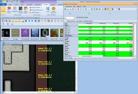
During the photolithography process in the wafer fab, the “critical dimensions” of various geometries on the device may need to be documented. The PAX-it! Image Analysis module allows the measurement of line widths and other features automatically and very repeatably. The CD Module measurement wizard may be used for images captured from the optical microscope or from SEM images, which may also be stored in the database and used for measurements and reports.
If you support a semiconductor fab or microelectronics manufacturing facility, a PAXit! software license bundled with a PAXcam digital microscope camera is the perfect toolset for you! The PAXit! and PAXcam family of products offers the following:
- Multiple high resolution cameras, for brightfield as well as low-light applications, to meet your specific needs and budget
- PAX-it! Image Database Software to manage your high-resolution images: search, annotate, and automatically create reports and documents
- Measure lines, angles, layers, critical dimensions, and more
- Create report templates for documentation — capture directly from the PAXcam to your report, or send marked and measured images with data to your report
- View the device features under your microscope in real time on your computer monitor
- Supports digital measurements, network site licensing, image analysis, Critical Dimension measurements, or remote consultation via live streaming — all through modular software components
- Optional upgrade to Motorized Microscope control, for automated inspection, measurement and analysis
PAX-it digital imaging software is used in semiconductor fabs and microelectronics manufacturing plants around the world. Contact us to request pricing information or to discuss the options you have with PAX-it!
Semiconductor- Microelectronics Images
Images taken with PAXcam cameras from various labs and samples.
NOTE: Images have been resized downward, and compressed, in order to present them as samples on the web. Original images are larger files and higher resolution.
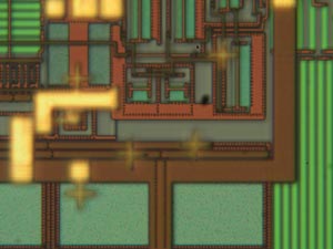
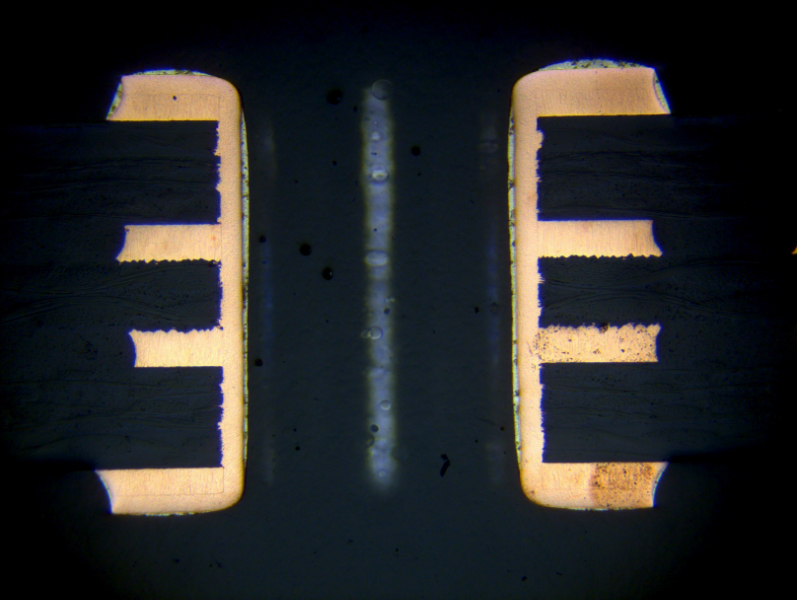
Microelectronics view
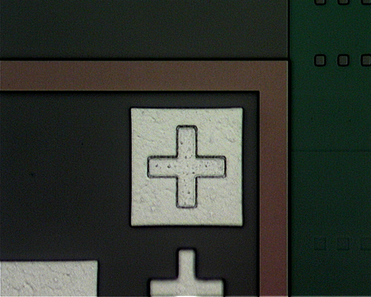
Microchip detail, reflected light compound microscope
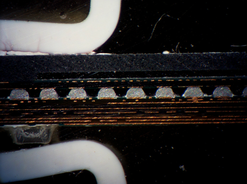
PAXcam1+; Stereozoom scope at 45x. 8-layer PCB, with an encapsulated ball-bonded microchip

PAXcam2+; CCD chip with capton layer coating
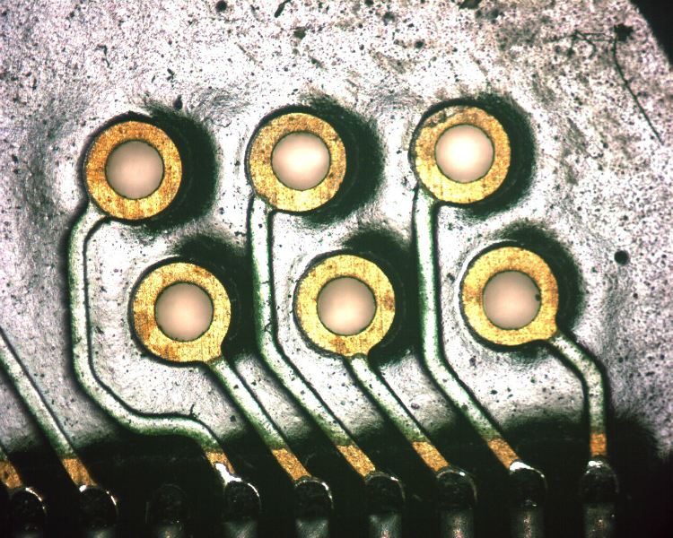
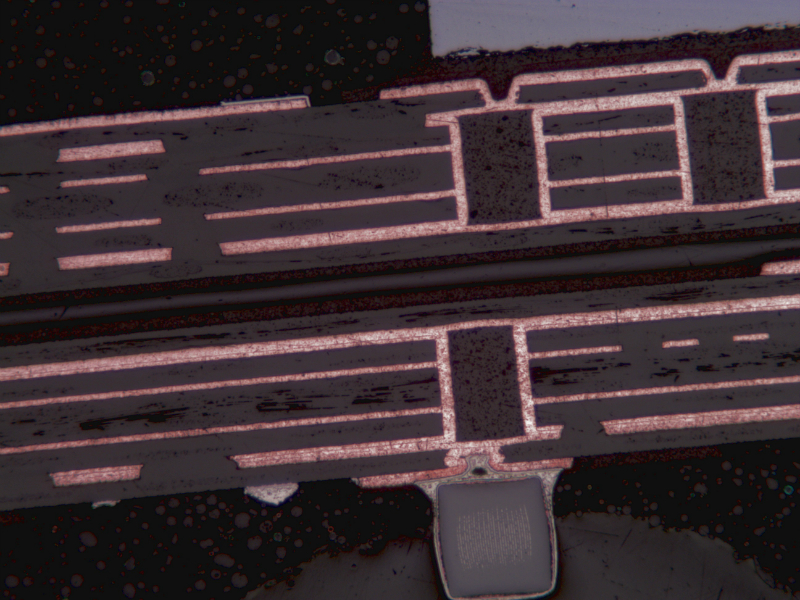
PAXcam2+; Circuit board thru hole cross section

PAXcam2; RFID integrated circuit
PAXcam5; Printed circuit board cross section
Microelectronics view
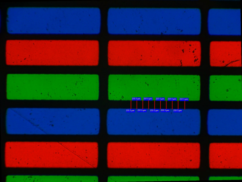
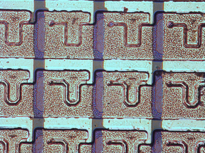
PAXcam2+; LCD-FPD; Critical Dimension measurements made with PAX-it CD Module